TSMC Dominance: How Nanometer Precision Drives Modern Tech
"The silicon chips inside your phone and the servers powering AI are no longer just components; they are the heartbeat of the modern economy."
Taiwan's semiconductor industry has transitioned from a specialized manufacturing hub to the indispensable architect of global computing power. Through massive scale and specialized precision, the island's foundry model dictates the pace of innovation for every major tech giant on Earth.
* TSMC maintains dominance by scaling process nodes and integrating high-performance computing capabilities. * The industry faces intense global competition alongside critical resource constraints like power and water. * The global semiconductor market offers massive growth potential but remains subject to intense cyclical volatility. * Maintaining a leading position requires robust international collaboration and massive R&D investment.
Why does one island dictate the global economy?
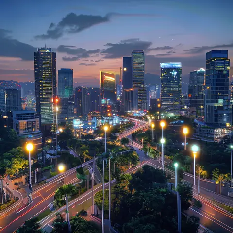
In the blue glow of midnight, a tired engineer taps a glass screen, feeling the warmth of a chip forged in a distant, sterile cleanroom.
At 2:00 AM in a quiet suburb, a designer taps a smartphone screen, unaware that the tiny circuit they are touching was likely etched in a cleanroom thousands of miles away. This connection between a single person's hand and a massive industrial complex is the foundation of the modern age.
By 2020, Taiwan had established itself as the unmatched leader of the global semiconductor industry, with TSMC alone accounting for more than 50% of the global market share.
This concentration of power means that the success of companies like Apple, Nvidia, and AMD is inextricably linked to the specialized processes happening in Taiwanese fabrication plants.
The shift from being a mere component provider to becoming the architect of advanced computing power has changed the industry's DNA. Leading-edge foundry services do not just manufacture chips; they enable the very existence of AI and high-performance computing.
Because these companies rely on TSMC's specialized nodes, the foundry's technological roadmap essentially becomes the global technology roadmap.
The relationship between the foundry and the end-product designer is a delicate dance of innovation. As designers push for more transistors in smaller spaces, the manufacturing process must evolve to meet them.
This symbiotic relationship ensures that as AI demand grows, the manufacturing capabilities must scale accordingly to prevent a global bottleneck. But the physical limits of silicon are starting to push back.
How big is the market and why does it shift so fast?
A shipping container moves through a busy port, carrying the value of a small nation's GDP in a single metal box. This is the physical reality of a market that moves billions of dollars across borders every single day.
The scale of this industry is staggering and has grown at an unprecedented pace. According to the Semiconductor Industry Association, sales of semiconductors reached a record $555.9 billion in 2021, representing a 26.2% increase over previous levels.
Within that massive global pool, sales in China reached $192.5 billion during that same period.
The industry is characterized by massive growth potential alongside significant cyclical volatility. While the demand for consumer electronics and industrial tools fluctuates, the underlying trend is toward higher complexity and higher value.
This volatility means that while the market can expand rapidly, it can also face sudden shifts based on consumer spending or supply chain disruptions.
To manage this scale, the global footprint of fabrication is expanding. While Taiwan remains the heart of the industry, there is an increasing push to distribute manufacturing capacity across the US and the Asia-Pacific region to mitigate risks.
This geographic spread is a response to the realization that the world's digital economy cannot rely on a single point of failure. However, as the chips get smaller, the engineering becomes much harder.
What happens when we hit the limits of physics?
A specialized cooling system hums loudly in a darkened laboratory, fighting to dissipate the heat generated by a massive array of processors. In the world of microchips, heat is the enemy of performance and the greatest challenge to scaling.
As traditional transistor scaling reaches its physical limits, the industry has turned to advanced packaging to push performance boundaries. It is no longer enough to just make transistors smaller; engineers must now find ways to stack them and connect them using sophisticated 3D structures.
This shift toward advanced packaging allows for greater computational density without solely relying on shrinking the silicon footprint.
The relentless pursuit of smaller process nodes introduces immense manufacturing complexity. Each step toward a smaller nanometer rating requires new materials, new light sources, and entirely new manufacturing techniques.
This complexity creates a high barrier to entry, protecting the leaders but also increasing the cost of failure.
Operational demands on these facilities are massive, particularly regarding power and water usage. A modern fabrication plant requires a constant, massive draw of electricity and millions of gallons of ultrapure water to clean silicon wafers.
Managing these resources is not just a matter of cost; it is a matter of operational survival. But as the machines get more complex, the threats to them become more sophisticated.
How do we defend the most valuable factories on Earth?
A security analyst stares at a monitor showing a sudden spike in network traffic, a digital fingerprint of an intrusion attempt. In the semiconductor sector, the battle for dominance is fought as much in cyberspace as it is in the physical world.
The industry faces increasing scrutiny and sophisticated cyber threats. According to Taiwan's Ministry of Justice Investigation Bureau (MJIB), there were over 2.4 million cyber intrusion attempts per day in 2024, which is double the volume recorded in 2023.
These attacks target intellectual property and operational stability, making cybersecurity a pillar of industrial defense.
The integration of Taiwan's semiconductor sector into the global high-tech infrastructure means that local stability is a matter of global economic security.
This geopolitical reality complicates the expansion of manufacturing, as companies must balance local production with the need to diversify their supply chains.
Sustaining growth amidst these constraints requires a delicate balance of political maneuvering and resource management. As the industry grows, the strain on local power grids and water supplies becomes more pronounced.
Leaders must navigate these local environmental and political pressures while maintaining the ability to meet global demand. This leads us to the ultimate driver: the AI revolution.
What does the AI era mean for the future of silicon?
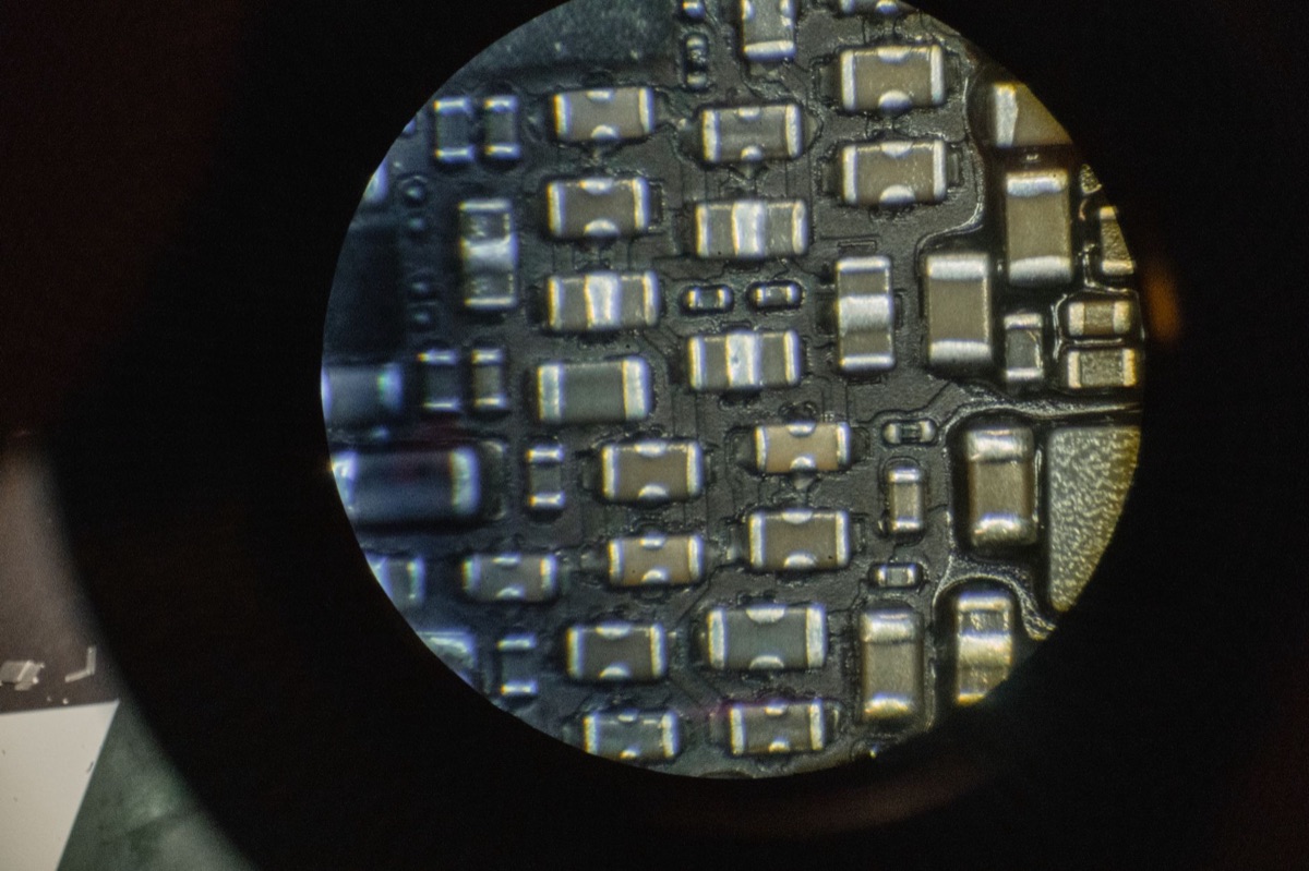
A researcher peers through a microscope, looking for a defect that is invisible to the naked eye. The race to own the next generation of AI-capable chips is the primary driver of current industrial investment.
The current boom is fueled by specific, massive demand drivers, most notably AI chip requirements. Large language models and generative AI require specialized chips with massive memory bandwidth and processing power.
This specialized demand is driving a new era of specialized silicon, where general-purpose chips are being replaced by application-specific architectures.
Maintaining technological superiority requires continuous, massive investment in R&D. The roadmap for the next decade is already being written, with companies investing billions to master the next generation of extreme ultraviolet lithography and atomic-layer deposition.
This is a race where being second often means being obsolete.
The global race to secure manufacturing capacity is intensifying. As nations realize that chips are the "new oil," they are racing to build domestic capabilities.
However, the specialized expertise required to run a leading-edge fab cannot be built overnight, ensuring that the current leaders remain central to the global economy for the foreseeable future.
| Feature | Traditional Manufacturing | Advanced Semiconductor Foundry |
|---|---|---|
| Primary Goal | Volume and Cost Efficiency | Performance and Precision |
| Key Resource | Raw Materials | Extreme Purity and Power |
| Complexity | Linear Scaling | Non-linear, Atomic-level Scaling |
| Market Driver | Consumer Goods | AI, HPC, and Data Centers |
- Identify the Node: Determine the specific process technology required for the target application.
- Secure the Supply: Establish deep partnerships with specialized equipment and material providers.
- Scale the Packaging: Integrate advanced 2.5D or 3D packaging to maximize chiplet performance.
- Manage the Environment: Implement robust water recycling and power-stabilization systems.
The semiconductor industry is a specialized field where success is measured in nanometers and success is often dictated by the ability to manage extreme complexity. While the growth is massive, the barriers to entry are equally high.
FAQ
What segment does TSMC primarily serve today? TSMC primarily serves the high-end market, providing advanced semiconductor manufacturing for the world's leading technology companies, including those focused on AI, mobile, and high-performance computing.
What are the primary operational challenges for a leading fabrication plant? The primary challenges include maintaining extreme environmental purity, managing massive power draws, and ensuring a constant supply of ultrapure water for wafer cleaning and cooling.
How volatile is the overall semiconductor market? The market is characterized by high growth potential but is subject to sudden shifts based on global consumer spending and supply chain disruptions.

Comments 0